
Gallium arsenide — properties, structure, and applications
Gallium arsenide (GaAs) is a III–V semiconductor with a direct bandgap. It is widely used in high-frequency electronics and optoelectronics, including LEDs, lasers, and solar cells.
Gallium arsenide is an inorganic compound of gallium and arsenic with the chemical formula GaAs. It belongs to the III–V family of semiconductors and combines elements from group III (gallium) and group V (arsenic). The bonding in GaAs has significant covalent character with partial ionic contribution: formally gallium is in a +3 oxidation state and arsenic in −3, but the real charge distribution is more complex. For a general reference see chemical compound.
Image gallery
4 Images

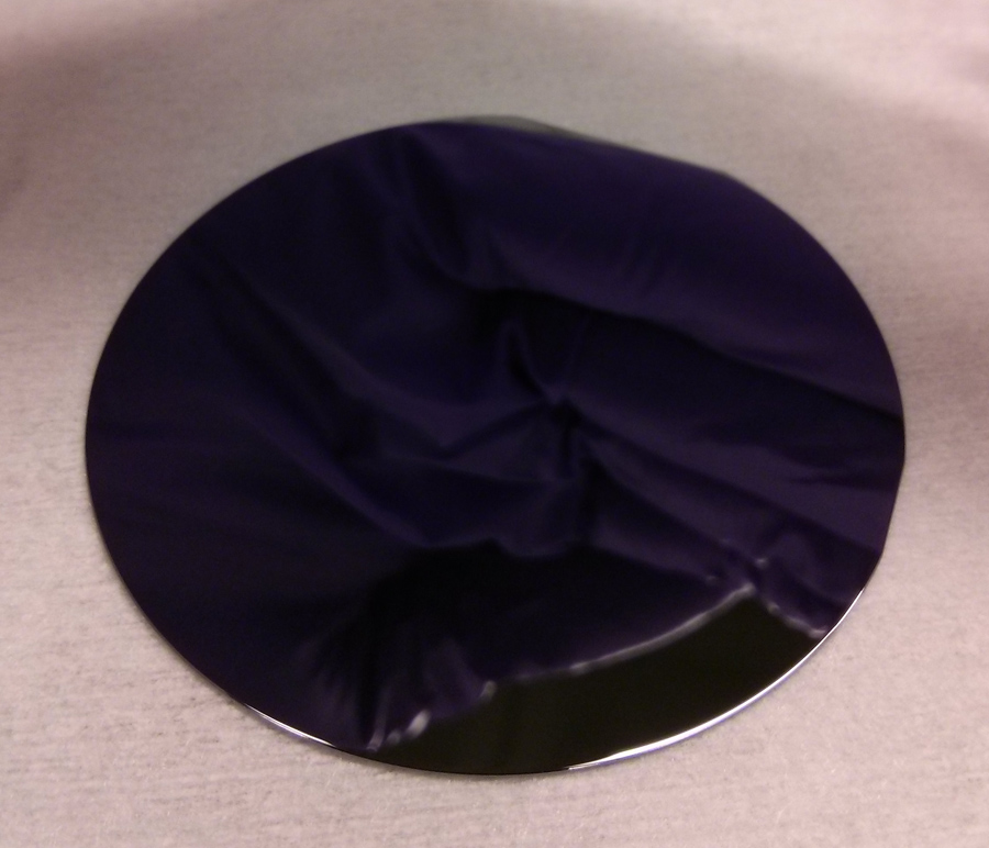

Crystal structure and electronic character
GaAs crystallizes most commonly in the zincblende (cubic) structure, which provides a direct electronic bandgap. This direct bandgap makes GaAs efficient at emitting and absorbing light, distinguishing it from indirect-gap semiconductors such as silicon. The material also offers higher electron mobility than silicon, which improves performance at high frequencies. For background on the constituent elements, see gallium and arsenide.
Preparation and processing
Single crystals and epitaxial films of GaAs are commonly produced by techniques such as molecular beam epitaxy (MBE) and metal-organic chemical vapor deposition (MOCVD). These methods enable precise control of composition, doping and heterostructure formation (for example AlGaAs/GaAs layers). Doping with donors or acceptors tailors the electrical conductivity for specific device functions. See also materials described as ions in ionic/covalent compounds.
Uses and applications
- Optoelectronics: light-emitting diodes (LEDs), laser diodes and photodetectors benefit from GaAs's direct bandgap.
- High-frequency electronics: microwave and millimeter-wave integrated circuits, radar and satellite transceivers exploit its high electron mobility.
- Solar cells: space-grade photovoltaic cells often use GaAs because of its radiation resistance and high efficiency.
- Research devices: heterostructures, quantum wells and high-electron-mobility transistors (HEMTs) are built using GaAs or related alloys.
Safety and notable facts
Arsenic compounds can be toxic, so synthesis and processing of GaAs require appropriate controls to limit exposure and environmental release. The material is also a foundation for many compound-semiconductor technologies and is often alloyed (for example with aluminum or indium) to tune electronic and optical properties. For more technical details on oxidation states and bonding, consult sources about the oxidation state of gallium in compounds.
Because of its combination of optical and electronic properties, GaAs remains important for specialized applications where performance at high frequency, high efficiency in light emission or resilience in space environments outweighs its higher cost relative to silicon.
Related articles
Author
AlegsaOnline.com Gallium arsenide — properties, structure, and applications Leandro Alegsa
URL: https://en.alegsaonline.com/art/37324