
Scanning electron microscope (SEM)
A scanning electron microscope uses a focused electron beam to image and analyze specimen surfaces, producing topographic, compositional, and structural information across many scientific and industrial fields.
Overview
A scanning electron microscope (SEM) is a type of electron microscope that forms images by scanning a surface with a focused beam of high‑energy electrons. When the beam interacts with a solid specimen it generates a variety of signals that carry useful information about surface morphology, composition, and other properties. SEMs are valued for their high depth of field, three‑dimensional appearance of images, and ability to couple imaging with elemental analysis.
Image gallery
10 Images



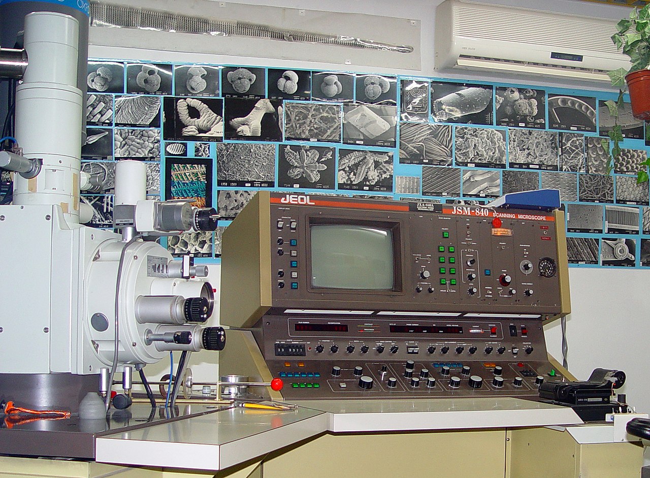


Key components and detected signals
An SEM comprises an electron source (gun), electromagnetic lenses and deflection coils to form and scan the beam, a vacuum chamber with a motorized stage, detectors, and electronics for image formation. Common signals used for imaging and analysis include:
- Secondary electrons: low‑energy electrons that provide fine surface topography with high spatial detail.
- Backscattered electrons: higher‑energy electrons that convey contrast related to atomic number and composition.
- Characteristic X‑rays: emitted when atoms are ionized; analyzed by EDS (energy‑dispersive X‑ray spectroscopy) to identify elemental composition.
- Other signals: Auger electrons, cathodoluminescence, and transmitted electrons in special SEM modes.
Sample preparation and operating modes
Because conventional SEM requires vacuum and can charge insulating samples, preparation often includes drying and coating specimens with a thin conductive layer (gold, carbon, or platinum). Specialized techniques—variable‑pressure or environmental SEM (VP/ ESEM) and cryo‑SEM—allow imaging of hydrated, nonconductive, or temperature‑sensitive samples with reduced preparation. Samples are mounted on conductive stubs and positioned so the beam can raster across regions of interest.
Resolution, contrasts and distinctions
SEMs resolve surface details at the nanometer to sub‑nanometer scale depending on instrument design and operating conditions. Compared with transmission electron microscopes (TEM), SEMs image surfaces directly and provide greater depth of field but generally lower ultimate resolution. Compared to light microscopy, SEMs deliver much higher magnification and surface detail.
History, applications, and notable capabilities
Developed during the mid‑20th century, SEMs became widely available as instruments and techniques advanced. Modern SEMs are indispensable across materials science, semiconductor inspection, metallurgy, biology, forensics, geology, and archaeology. Typical uses include failure analysis, particle and fiber characterization, microstructure examination, and correlative studies combining imaging with elemental mapping. Recent developments enable in‑situ experiments (heating, mechanical testing) and automated high‑throughput imaging for research and industrial quality control.
Limitations and practical considerations
Limitations include the need for vacuum (for many modes), possible beam damage to sensitive samples, and the need for conductive paths to ground. Operators balance beam energy, working distance, and detector choice to optimize contrast and resolution for each specimen. With appropriate technique selection and sample preparation, SEMs provide a versatile platform for visualizing and analyzing surfaces at microscopic to nanoscopic scales.
Related articles
Author
AlegsaOnline.com Scanning electron microscope (SEM) Leandro Alegsa
URL: https://en.alegsaonline.com/art/87770