
Nanoelectromechanical systems (NEMS)
Nanoelectromechanical systems are devices that integrate electrical and mechanical functions at nanometer scales, offering high sensitivity and frequency for sensing, signal processing and fundamental research.
Nanoelectromechanical systems (NEMS) are devices that combine electrical and mechanical components at nanometer dimensions. They are the nanoscale continuation of microelectromechanical systems (MEMS), but their tiny size gives them distinct behavior: very low mass, very high resonance frequencies, and a high surface-to-volume ratio. Those differences enable exceptional sensitivity and new functions, while also introducing physical phenomena absent at larger scales.
Image gallery
3 Images
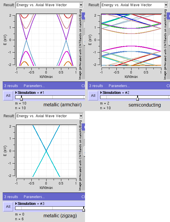

Core characteristics
- Scale and materials: Structures range from a few nanometers up to a few hundred nanometers and are made from silicon, silicon carbide, carbon nanotubes, graphene, and other nanomaterials.
- Mechanical elements: Cantilevers, beams, plates and resonators are common; moving parts may be only a few atoms thick.
- High frequencies and low mass: Reduced dimensions raise natural frequencies into the MHz–GHz range, improving temporal resolution and bandwidth.
- Surface-dominated physics: Surface forces, adhesion, van der Waals and Casimir interactions, as well as surface chemistry, strongly influence behavior.
Fabrication uses both top-down patterning (electron-beam and advanced lithography, etching) and bottom-up assembly (chemical synthesis of nanotubes and graphene). Electrical readout methods include capacitive, piezoresistive, optical and tunneling techniques, often combined with integrated electronics for signal conditioning.
History and development
NEMS evolved from MEMS research in the late 20th and early 21st centuries as fabrication and characterization techniques reached the nanoscale. Early demonstrations adapted micromechanical resonators and sensors to ever-smaller dimensions, while progress in carbon-based nanomaterials opened new device geometries. Laboratory prototypes gradually explored switching elements, resonant sensors and components for radio-frequency signal processing.
Applications and examples
NEMS are pursued for ultra‑sensitive mass, force and displacement sensing, where tiny added masses shift resonance frequencies. They appear in experimental high‑frequency filters and oscillators for communications, in switches that promise lower energy use than conventional transistors, and as components in scientific instruments that probe fundamental physics. Notable examples include nanoscale resonators used to detect nanoparticles or biomolecules, and beam or tube structures employed as ultra‑small accelerometers or pressure sensors.
Challenges and research directions
- Stiction and reliability: Adhesive forces can cause parts to stick, limiting repeatability and lifetime.
- Dissipation and noise: Energy loss and thermal (Brownian) motion set limits on sensitivity; improving quality factor (Q) is an active area.
- Integration: Combining NEMS with control electronics, packaging and scalable manufacturing remains difficult.
- Quantum and surface effects: At the smallest scales, quantum fluctuations and modified material properties require new models and measurement techniques.
Researchers are addressing these issues through surface engineering, novel materials, improved fabrication and hybrid approaches that mix top‑down and bottom‑up methods. For technical reviews and updates on device concepts and fabrication, see further reading.
Related articles
Author
AlegsaOnline.com Nanoelectromechanical systems (NEMS) Leandro Alegsa
URL: https://en.alegsaonline.com/art/68267