
Scanning tunneling microscope
An instrument that images and manipulates conductive surfaces at atomic scale by measuring electron tunneling. Widely used in surface science, spectroscopy, nanotechnology and atomic-scale fabrication.
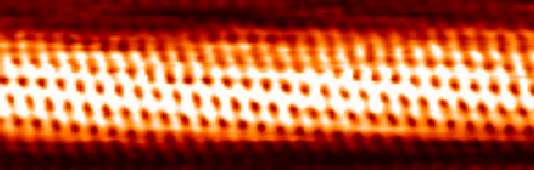
The scanning tunneling microscope (STM) is an instrument that can image and, in some cases, manipulate surfaces with atomic-scale resolution. It operates by bringing an extremely sharp conductive tip very close to a sample surface—often a few angstroms—and measuring the tiny electrical current that flows by quantum mechanical tunneling when a bias voltage is applied. Variations in the tunneling current are converted into a map of the surface that reveals atomic positions and electronic structure.
Image gallery
8 Images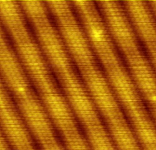



Principle and main components
STM relies on the quantum tunneling effect: electrons can tunnel across the narrow vacuum gap between tip and sample when they are very close. The main components include a sharp conductive tip, a piezoelectric scanner to control sub-nanometre movements in x, y and z, a low-noise current amplifier that detects picoampere-level currents, and control electronics and software to raster-scan the tip or sample and build images.
Modes of operation and spectroscopy
Two common imaging modes are constant-current mode—where the tip height is adjusted to keep the tunneling current constant, producing a topographic image—and constant-height mode—where current variations are recorded at fixed height for faster imaging. Scanning tunneling spectroscopy (STS) measures current as a function of bias voltage at a fixed position, providing information about the local electronic density of states and energy-resolved features such as surface states and band gaps.
History and recognition
The modern STM was developed at IBM's Zurich research laboratory in the early 1980s by Gerd Binnig and Heinrich Rohrer; their work transformed surface science and earned them the Nobel Prize in Physics in 1986. Original publications and institutional records can be consulted via primary archives and retrospectives related to the invention.
Applications
STM is widely used to study atomic arrangements, point defects, step edges, adsorbates and low-dimensional materials such as surfaces of metals, semiconductors and two-dimensional crystals. It enables local spectroscopy, imaging of electronic inhomogeneity, and, under carefully controlled conditions, manipulation of individual atoms and molecules to assemble nanoscale structures.
Variants and related techniques
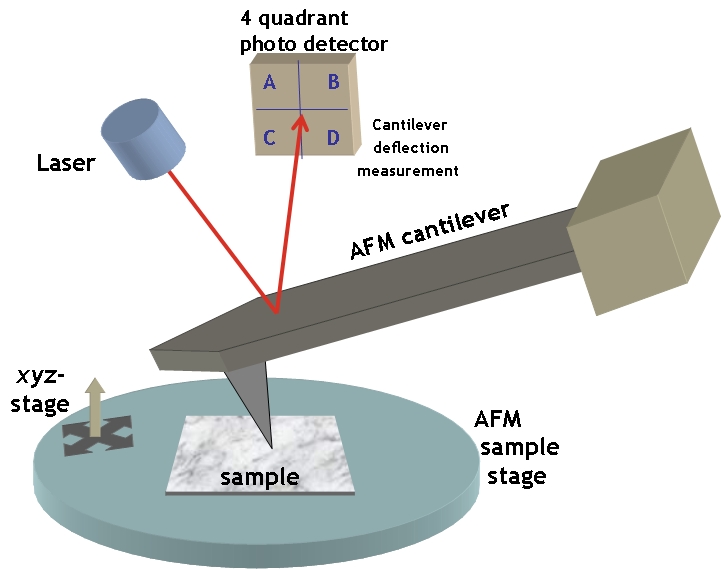
Several variants extend STM capabilities: spin-polarized STM can probe magnetic structure, and inelastic tunneling spectroscopy can detect vibrational excitations of adsorbed molecules. Atomic force microscopy (AFM) is a related technique that can image insulating surfaces by sensing forces rather than tunneling currents.
Limitations and practical considerations
STMs require electrically conductive or semiconducting samples and are sensitive to vibration, acoustic noise, temperature drift and surface contamination. To achieve the best resolution, instruments are often operated in ultra-high vacuum and at low temperatures. Image contrast depends not only on geometric topography but also on the electronic structure of tip and sample, so interpretation requires care and, where possible, complementary measurements.
Quality of the tip—its sharpness, material and cleanliness—strongly affects image fidelity. Routine sample preparation, careful control of the experimental environment, and appropriate choice of imaging mode are essential for reliable data. STM continues to be a foundational tool in nanoscience and surface physics, providing both qualitative images and quantitative local electronic information for research and technology development.
Questions and answers
Q: What is scanning tunneling microscopy?
A: Scanning tunneling microscopy (STM) is a way to view the shape of tiny objects. It can make pictures of atoms on a surface and move the atoms to different places.
Q: Who invented STM?
A: STM was invented by Gerd Binnig and Heinrich Rohrer in 1981 at IBM, in Zürich.
Q: When did they invent it?
A: They invented it in 1981 at IBM, in Zürich.
Q: What can STM do?
A: STM can make pictures of atoms on a surface and move the atoms to different places.
Q: Did they win an award for inventing STM?
A: Yes, they won the Nobel Prize in Physics for inventing it in 1986.
Q: Where did they win this award?
A: They won the Nobel Prize in Physics for inventing it in 1986.
Q: What year did they win this award?
A: They won the Nobel Prize in Physics for inventing it in 1986.
Related articles
Author
AlegsaOnline.com Scanning tunneling microscope Leandro Alegsa
URL: https://en.alegsaonline.com/art/87771