Photolithography: Light-driven patterning for printing and semiconductor manufacturing
Photolithography uses light and photosensitive materials to transfer patterns onto surfaces, from mass photographic printing to microfabrication of semiconductor devices.
Photolithography is a process that uses light to transfer a pattern from a mask or negative onto a substrate coated with a light-sensitive material. In its broadest sense it combines principles of photography and lithography, allowing precise reproduction of images and geometric shapes. The technique ranges from large-format printing of images to the microscopic patterning required for electronic circuits.
Image gallery
10 Images


Core components and how it works
At its simplest, photolithography requires a light source, a patterned mask (often called a photomask), a substrate, and a photosensitive coating (photoresist). Light passes through or reflects from the mask and exposes the photoresist in a controlled pattern. Subsequent chemical development removes either the exposed or unexposed resist (depending on whether it is positive or negative resist), creating a durable pattern that can be used for etching, deposition, or lift-off processes.
Characteristics and common variants
- Resolution: Determined by wavelength of the light and optical system; shorter wavelengths enable finer features.
- Photoresists: Formulated for sensitivity, contrast, and resistance to downstream processing.
- Exposure systems: Range from simple contact printers to sophisticated projection steppers and scanners used in microfabrication.
- Mask types: Transparent masks with opaque patterns or phase-shifting masks improve fidelity at small scales; see photomask technology for details.
Historically, photolithography evolved from 19th-century photographic and printmaking practices and was adapted in the mid-20th century to meet the needs of electronics manufacturing. As integrated circuits proliferated, photolithography became the central patterning method for producing integrated circuits, enabling repeated, high-throughput replication of microscopic circuit features across wafers. Advances in optics, resist chemistry, and stage control drove the industry toward progressively smaller feature sizes.
Applications and importance
Beyond semiconductor fabrication, photolithography is employed in mass printing of images and fine graphics, microelectromechanical systems (MEMS), printed circuit boards, and the production of microfluidic devices. In commercial printing contexts it enables efficient mass printing of photographic and graphic content with high fidelity. In microfabrication, it is the foundational step that defines device geometry and density.
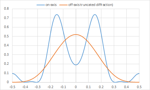
Notable distinctions include the difference between optical photolithography used for micron- and submicron-scale features and specialized variants such as electron-beam or X-ray lithography for extreme-resolution needs. Practical limitations arise from diffraction, alignment precision, and resist chemistry, so ongoing research focuses on new light sources, immersion techniques, multiple-patterning strategies, and novel materials to extend capability.
Photolithography remains a versatile and widely used patterning method because it combines speed, reproducibility, and compatibility with many materials and processes, making it indispensable in both large-scale printing and the layered manufacturing of modern electronics.
Questions and answers
Q: What is photolithography?
A: Photolithography is the combination of photography and lithography.
Q: What are the uses of photolithography?
A: The uses of photolithography include mass printing of photographs and making integrated circuits.
Q: What is microphotolithography?
A: Microphotolithography is the use of photolithography to transfer geometric shapes on a photomask to the surface of a semiconductor wafer for making integrated circuits.
Q: What is the difference between photolithography and lithography?
A: Photolithography is a combination of photography and lithography whereas just lithography is the process of creating patterns on a surface using a chemical treatment.
Q: How is photolithography used for making integrated circuits?
A: Photolithography is used to transfer geometric shapes on a photomask to the surface of a semiconductor wafer for making integrated circuits.
Q: Can photolithography be used for mass printing of photographs?
A: Yes, photolithography can be used for mass printing of photographs.
Q: What is the significance of photolithography?
A: Photolithography has a significant role in the manufacturing of integrated circuits and mass printing of photographs. It is a widely used process in the semiconductor industry.
Related articles
Author
AlegsaOnline.com Photolithography: Light-driven patterning for printing and semiconductor manufacturing Leandro Alegsa
URL: https://en.alegsaonline.com/art/76603