MOSFET — metal–oxide–semiconductor field‑effect transistor
MOSFET: a voltage‑driven semiconductor device used as a switch or amplifier. Covers structure, operation, history, common variants, and major applications in electronics and power systems.
Overview
A MOSFET (metal–oxide–semiconductor field‑effect transistor) is a type of transistor that controls electrical current using an electric field. It is a foundational electronic component in modern circuitry and most commonly functions as an electrically controlled switch. MOSFETs appear throughout consumer electronics, computing hardware and power conversion equipment. While some MOSFETs are optimized to amplify analog signals, the majority operate as on/off elements in digital logic and switching systems.
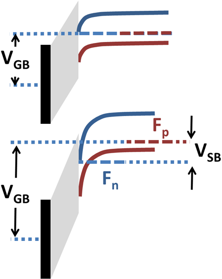
Image gallery
10 Images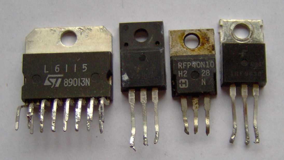
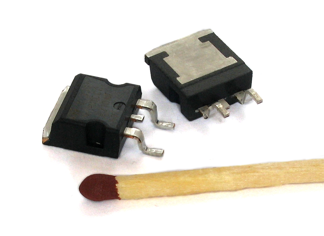


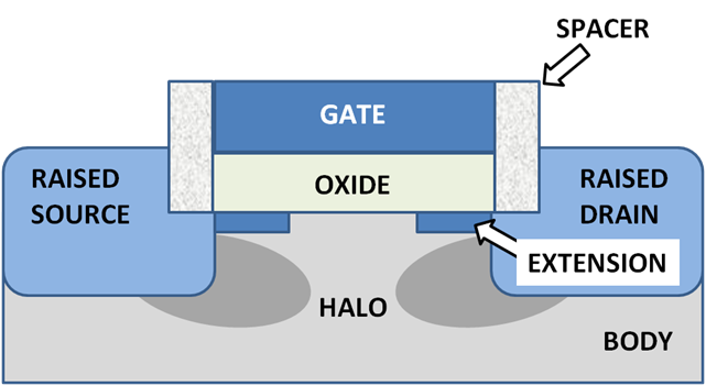

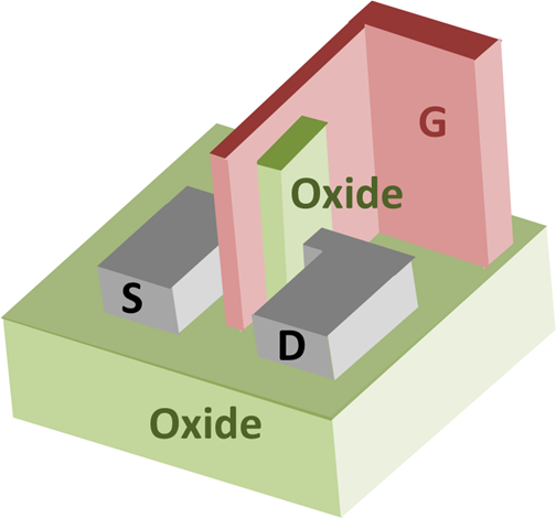
Structure and operation
Physically, a MOSFET has three main terminals: gate, source and drain. The gate terminal is separated from the semiconductor body by a thin insulating layer of oxide; applying a voltage to the gate modifies the charge distribution in the semiconductor channel and thereby controls current between the source and drain. This field‑effect principle places MOSFETs in the broader family of transistors, but their metal‑oxide‑semiconductor construction gives them distinctive characteristics such as very high input impedance and fast switching capability. Designers often model a MOSFET as a voltage‑controlled resistor or switch when used in digital circuits.
Key parts and parameters
- Gate: the control electrode that establishes the channel.
- Source and drain: the terminals through which carriers enter and leave the channel.
- Oxide layer: the thin insulating film that isolates the gate and enables field control.
- Threshold voltage: the gate voltage at which a conducting channel forms.
Performance is often described by on‑resistance, threshold voltage, switching speed and maximum current. In integrated circuits, MOSFETs are fabricated together with other devices on a semiconductor wafer; they are the workhorse elements of modern computers and logic circuits.
History and development
The MOSFET evolved from earlier transistor technologies and became practical after advances in oxide growth and fabrication techniques. Its invention and subsequent refinement enabled the dense integration of transistors on silicon chips, leading to rapid miniaturization and increased circuit complexity. Over decades, scaling and process innovations have allowed vastly larger numbers of transistors to be placed on a single integrated circuit, enabling higher performance and lower cost per function. MOSFET variants and process nodes continue to evolve to meet demands for speed, power efficiency and density.
Applications and examples
MOSFETs are ubiquitous. In digital electronics they form the switching elements of CMOS logic families and microprocessors. In analog and power electronics they serve in amplifiers, DC–DC converters and motor controllers. Common application categories include:
- Analog signal processing — low‑noise front ends and small‑signal amplifiers.
- Digital logic — gates, memories and processors.
- Power switching — efficient converters, inverters and motor drives.
Variants and notable facts
There are many MOSFET types: enhancement and depletion modes, n‑channel and p‑channel polarities, as well as specialized power MOSFETs and lateral or vertical structures optimized for integration or high current handling. The name itself describes the layered construction — metal (gate), oxide (insulator) and semiconductor (channel and contacts). Most MOSFETs are manufactured as part of complex integrated circuits, and the device has been central to the exponential growth in processing capability that characterizes modern electronics.
Because MOSFETs switch with voltage rather than current, they offer high input impedance and low drive power, but designers must manage issues like gate charge, thermal dissipation and protective measures against static and transient voltages. Understanding these tradeoffs is essential for applying MOSFET technology effectively in both small‑signal and high‑power systems.

History
The functional principle of MOSFETs is about 20 years older than that of the bipolar transistor. The first patent applications date back to 1926 by Julius Edgar Lilienfeld and 1934 by Oskar Heil. However, the first MOSFETs were not manufactured until 1960, when silicon/silicon dioxide became available as a material system with which a reproducibly good semiconductor-insulator interface could be produced. This was associated with a move away from germanium as the base material and increasing demands on the manufacturing conditions (clean rooms, strict temperature regime).
From the beginning or middle of 1970, doped polysilicon was used as a gate material, replacing evaporated aluminium. Since the turn of the millennium, there has been increased research into the new high-k+metal gate technology, which was used in mass production for the first time in 2007.
Name
The name metal-oxide semiconductor field-effect transistor derives from the original layer sequence of the gate layer stack. Until the early 1980s, the use of aluminum (a metal) as the gate material dominated, separated from the conductive channel in the silicon substrate (semiconductor) by a non-conductive silicon dioxide layer (insulator). In the 1980s, processes using doped polysilicon as the gate material became increasingly common. This is still the most common design of commercially available CMOS circuits. Since no metal is used, the designation MOSFET is no longer correct, but is still used as a synonym.
With increasing miniaturization, MOS transistors with polysilicon gate show electrical disadvantages, because a depletion region forms in the gate with certain circuits (polysilicon depletion). Therefore, research into alternative gate materials (e.g. transition metals) has been carried out since the early 2000s. In parallel, research was also conducted into alternative insulator materials with high dielectric constant (so-called high-k materials) in order to reduce the increasing leakage currents. In 2007, Intel was the first manufacturer to introduce the combination of both changes (cf. high-k+metal gate technology); several other manufacturers of high-performance processors followed. In these cases the designation MOSFET is therefore correct again, nevertheless it is often more convenient to use the neutral designation MISFET (metal-non-conductor-semiconductor FET) or more generally IGFET (FET with insulated gate).
Questions and answers
Q: What is a MOSFET?
A: A MOSFET is a metal-oxide-semiconductor field-effect transistor, which is an electronic component that acts as an electrically controlled switch.
Q: What are transistors used for?
A: Transistors are small electrical devices that are used in radios, calculators, and computers; they are some of the most basic building blocks of modern electronic systems.
Q: How does a MOSFET work?
A: A MOSFET acts like a valve for electricity. It has one input connection (the "gate") which is used to control the flow of electricity between two other connections (the "source" and "drain"). The gate acts as a switch that controls the two outputs.
Q: What does the name 'MOSFET' refer to?
A: The name MOSFET describes the structure and function of the transistor. 'MOS' refers to the fact that it is built by layering metal (the "gate") on oxide (an insulator which prevents the flow of electricity) on semiconductor (the "source" and "drain"). 'FET' describes the action of the gate on the semiconductor.
Q: Where are almost all MOSFETS used?
A: Almost all MOSFETS are used in integrated circuits.
Q: How many transistors can be fit onto an integrated circuit today compared to 1970?
A: As of 2008, it is possible to fit 2,000,000,000 transistors on a single integrated circuit whereas in 1970 around 2,000 could be fitted onto one IC.
Related articles
Author
AlegsaOnline.com MOSFET — metal–oxide–semiconductor field‑effect transistor Leandro Alegsa
URL: https://en.alegsaonline.com/art/66845