Graphene: the two-dimensional form of carbon
Graphene is a single-atom-thick sheet of carbon with a hexagonal lattice. It combines exceptional strength, conductivity and flexibility, and underpins advances in electronics, composites, sensing and energy storage.
Overview
Graphene is a single layer of carbon atoms arranged in a flat, hexagonal lattice. As an atomically thin sheet it is described as a two-dimensional material; this atomic-scale thinness gives graphene properties that differ sharply from bulk forms of carbon. Graphene is the building block for several three-dimensional allotropes: stacking many sheets produces graphite, and other curved or closed forms relate to structures such as fullerenes and carbon nanotubes. Because it is the fundamental 2D layer, graphene is often contrasted with other carbon allotropes such as diamond or charcoal, which have very different bonding and bulk structures.
Image gallery
10 Images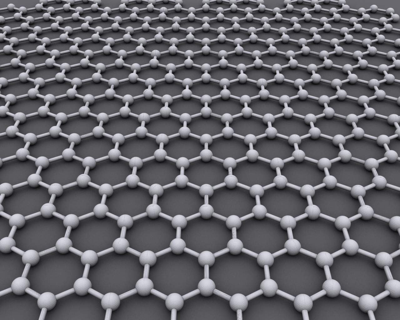


Structure and key properties
At the atomic level graphene is a single sheet of sp2-hybridized carbon atoms bonded in a repeating honeycomb, or "chicken wire", pattern. This regular arrangement is a specific kind of crystal structure that produces exceptional mechanical, electronic and thermal characteristics. Electrons in graphene behave as if they are massless over certain energy ranges, contributing to very high electrical conductivity. The same network also yields extraordinary tensile strength and flexibility for an ultrathin material, while remaining lightweight and highly permeable to certain chemical species.
Because graphene is strictly one atomic layer thick, it is categorized as a two-dimensional material in the sense used by condensed-matter physics. Stacked layers restore many bulk behaviors: many graphene sheets together form macroscopic three-dimensional solids like graphite, with interlayer forces and different electronic bands. The contrast between the single-layer and multilayer forms is central to how graphene is studied and applied.
History and discovery
The name "graphene" was introduced by Hanns-Peter Boehm in the 1960s by combining "graphite" and the chemical suffix '-ene' to indicate a sheet of conjugated carbon bonds. Experimental isolation and characterization of stable, free-standing graphene layers at ambient conditions were demonstrated in the 2000s; this work led to the 2010 Nobel Prize in Physics awarded to Andre Geim and Konstantin Novoselov for experiments on the two-dimensional material. Their methods and measurements established graphene as a distinct, reproducible form of carbon worthy of intensive research.
Applications and examples
Graphene's unusual combination of properties has prompted exploration across many fields. Common and emerging areas include:
- Electronics: high-mobility channels, transparent conductive films and potential use in flexible devices.
- Composites: reinforcing polymers, metals or ceramics to improve strength-to-weight ratios and conductivity.
- Sensors and membranes: sensitive chemical or biological detectors and atomically thin filtration layers.
- Energy: electrodes for batteries and advanced devices such as supercapacitors, as well as components in solar and thermal management systems.
Distinctions and notable facts
Graphene should not be confused with other carbon materials that may share elements of its structure but behave differently. For example, although graphene sheets can be rolled or curved to form structures related to carbon nanotubes or wrapped into closed cages resembling fullerenes, the electronic and mechanical behavior changes with curvature, defects and stacking. The characteristic hexagonal lattice is often described with the image of a honeycomb, emphasizing both symmetry and the two-atom basis of the unit cell. Practical production, large-area uniformity, and integration into devices remain active engineering challenges even as laboratory demonstrations show a wide range of possible uses.


Structure
All carbon atoms of graphene are sp2-hybridized, which means that each carbon atom can form three equivalent σ-bonds to other C atoms. This results in a honeycomb structure also known from the layers of graphite. The carbon-carbon bond lengths are all equal and are 142 pm. The third, non-hybridized 2p orbitals are perpendicular to the graphene plane, as in graphite, and form a delocalized π-bond system.
Consequently, graphene consists of two equivalent sublattices A and B, to which the carbon atoms are assigned. The sublattices are shifted with respect to each other by the bond length  The diatomic unit cell is
  spanned by the lattice vectors
  and In this case, these point to the neighbors next but one in each case. The length of the vectors and thus the lattice constant
  can be calculated to
 .
.
Graphene can be understood as a single crystal on the one hand, and as a giant molecule on the other. Similarly, smaller molecules such as benzene, hexabenzocoronene or naphthalene can be seen as hydrogen-substituted graphene fragments.
Properties
| Properties of graphene | |
| Property | Value |
| Mass per unit area | 7,57 × 10⁻⁷ kg-m-2 |
| E-modulus | approx. 1020 GPa |
| Tensile strength | 125 GPa |
| attenuation of visible light | 2,3 % |
| Layer thickness | 3,35 × 10⁻¹⁰ m |
| Thermal conductivity | approx. 5000 W/(m-K) |
| Electrical resistivity | 31 Ω |

Graphene has unusual properties that make it interesting for both basic research and applications, especially in physics.
For example, graphene face single crystals are exceptionally stiff and strong within the faces. Its modulus of elasticity of about 1020 GPa is equal to that of normal graphite along the basal planes and almost as large as that of diamond. Its tensile strength of 1.25×10¹¹ Pa is the highest ever determined and about 125 times that of steel. A ribbon of graphene 1 m wide and 3.35 × 10⁻¹⁰ m thick, that is, of one atomic layer, has therefore a tensile strength of 42 N. A ribbon for a space elevator made of graphene with a constant cross-sectional area would only be loaded to 87.3% of its tensile strength at the geostationary orbit altitude of 35,786 km.
Assuming monocrystalline graphite with a density of 2260 kg-m-3 and a layer spacing of 3.35 × 10⁻¹⁰ m, multiplication calculates a mass per unit area for graphene of 7.57 × 10⁻⁷ kg-m-2. One square kilometer thus weighs 757 g. "A graphene hammock one square meter in size could support a four-kilogram cat - and itself weigh only as much as a single cat whisker."
Graphene behaves as an electrical conductor due to the lack of a band gap, see the figure below for the energy of electrons in graphene. However, an artificial band gap in graphene can be created by "cutting" a so-called gate into the layer with a maximum width of 10 nm.
Measurements have shown that a single graphene layer attenuates light by about πα ≈ 2.3% (with fine structure constant α), over the entire visible spectrum.
Pseudo-relativistic behaviour
The electrical properties of graphene can be well described by a tight-binding model. Within the framework of this model, the energy of electrons with wavenumber  (see wave vector) to
 ,
,
With the nearest-neighbor hopping energy γ  and the lattice constant
  . Conduction and valence bands correspond to plus and minus signs, respectively, in the dispersion relation above. They touch each other in graphs exactly in six distinguished points, called K-points, but only two of them are independent (the rest are equivalent to these two by lattice symmetry). In their vicinity, the energy depends linearly on (cf. photon:
  ). Since the basis is diatomic, the wave function even has a formal spinor structure. This leads to the fact that electrons at low energies can be described by a relation equivalent to the Dirac equation, and additionally in the so-called chiral limit, i.e. for vanishing mass
  , which gives some special features:

Here denotes  the Fermi velocity in graphs, which takes the place of the speed of light;
  denotes the Pauli matrices, ψ
  the two-component wave function of electrons, and
  their energy.
Unusual quantum Hall effect
Because of the peculiarities in dispersion, in this material the staircase structure of the integer quantum Hall plateaus, σ  , for all stages exactly "shifted by 1/2",
  The two-valley structure (formal "pseudospin") and the "real" spin degeneracy together add up to an additional factor of 4. Remarkably, unlike the conventional quantum Hall effect, this can be observed even at room temperature.
Stiffness and temperature dependence
Graphene is extremely stiff in the layer direction because the sp2 bond between neighbouring atoms is comparable in strength to the sp3 bond of diamond. Accordingly, it is generally expected - and this corresponds to the experiment - that the properties of graphene which are of interest for applications are not only valid at absolute temperature zero, i.e. at -273.15 °C, but remain valid at room temperature.
One such property is thermoelectricity: a temperature gradient in graphene planes causes an electric field strength due to a decoupling of the temperature of the electrons from that of the lattice. Electric voltage when graphene is illuminated had been observed before, but the cause was thought to be photovoltaics. The fact that the decoupling can still be observed at room temperature is due to the rigidity of the lattice: the elementary vibrational excitations of the lattice (phonons) are so high-energy that the electrons rarely produce such a phonon.
Elastic behaviour and pseudo magnetic field
In July 2010, a publication in the American scientific journal Science reported extremely strong pseudo-magnetic fields. By elastic deformation, tiny triangular bubbles of 4 nanometers to 10 nanometers in size were created in graphene, in which the electrons moved as if a magnetic field of about 300 teslas was acting on them. It turned out that, unlike the effect of a real magnetic field, the observed effect does not affect the actual spin of the electron, but instead affects the pseudo-spin just mentioned, which is related to the existence of two different equivalent base atoms in the honeycomb structure. This pseudospin has a similar interaction with the pseudomagnetic field as real spins have with real magnetic fields, because these also generate "two-level systems". The experiments around the "pseudo-quantum Hall effect" generated in this way were based on theoretical predictions, which were thus confirmed.
Spin streams
In April 2011, A. Geim and coworkers published an article describing strong spin currents and current-induced magnetism near the Dirac point, i.e., near the meeting point of the conduction band and the valence band. This opens up the prospect of applications in spintronics.
Chemical functionalization and large-scale EU project
In 2013, the EU announced a major new project ("flagship project") on graphene, on which researchers in many Member States will collaborate, especially physicists and chemists. It is possible, for example, to "break" double bonds in graphene - every second bond is such a bond - and replace them with two single bonds, to which various organic molecules can then be attached: this allows the properties of the system to be specifically influenced.
Hydrodynamic behaviour with unusual properties
In 2016, a so-called hydrodynamic ("liquid-like") behaviour of the electrons in graphene was found, but with extraordinary properties: For example. the Wiedemann-Franz law, otherwise valid for metallic systems, that the ratio of thermal and electrical conductivity divided by the Kelvin temperature T is equal to a universal constant in metallic systems, is violated in graphene, in that when the Fermi energy approaches the overlap point, the thermal conductivity becomes much too large (i.e. the specific thermal resistance becomes much too small). Moreover, in this electron fluid (technical term: Dirac fluid) one observes an unusual tendency to form vortex structures.


Questions and answers
Q: What is graphene?
A: Graphene is one of the forms of carbon, with a two-dimensional honeycomb or 'chicken wire' structure made up of carbon atoms and their bonds.
Q: How is graphene related to graphite?
A: Graphite is many graphene sheets stacked together - three million graphene sheets stacked to form graphite would be only one millimetre thick.
Q: Who coined the term 'graphene'?
A: The term 'graphene' was coined as a combination of graphite and the suffix '-ene' by Hanns-Peter Boehm in 1962.
Q: What did Sir Andre Geim and Sir Konstantin Novoselov win the Nobel Prize in Physics for 2010 for?
A: Sir Andre Geim and Sir Konstantin Novoselov won the Nobel Prize in Physics for 2010 "for groundbreaking experiments regarding the two-dimensional material graphene".
Q: What are some possible applications of graphene?
A: Possible applications of graphene include supercapacitors.
Q: What other forms or allotropes does carbon have besides graphene?
A: Other forms or allotropes that carbon has besides graphene include diamonds, graphite, charcoal, fullerene and carbon nanotubes.
Related articles
Author
AlegsaOnline.com Graphene: the two-dimensional form of carbon Leandro Alegsa
URL: https://en.alegsaonline.com/art/40345
Sources
- doi.org : 10.1351/pac199466091893
- doi.org : 10.1002/zaac.19623160303
- nobelprize.org : Nobel Foundation announcement · webcitation.org
- bbc.co.uk : BBC News - Miracle material graphene can distil booze, says study
- bbc.co.uk : bbc.co.uk/news/science-environment-30246089
- sciencemag.org : sciencemag.org/content/346/6213/1092
- bbc.co.uk : bbc.co.uk/news/science-environment-20975580