Binary adder: digital circuits for adding binary numbers
An overview of binary adders: half and full adders, ripple-carry and faster designs, gate-level implementation, example additions, and their role inside processors and arithmetic units.
Overview
A binary adder is a digital circuit that computes the sum of binary numbers. At the simplest level an adder operates on single bits and a possible incoming carry, producing a sum bit and an outgoing carry. Multiple single-bit adders are combined to add multi-bit binary values, forming the basis of integer addition inside central processing units, arithmetic logic units, and many digital systems. For background on the numbering system used in these circuits see binary numbers and for context on their use in computing systems see computers.
Image gallery
5 Images

Basic components and how they work
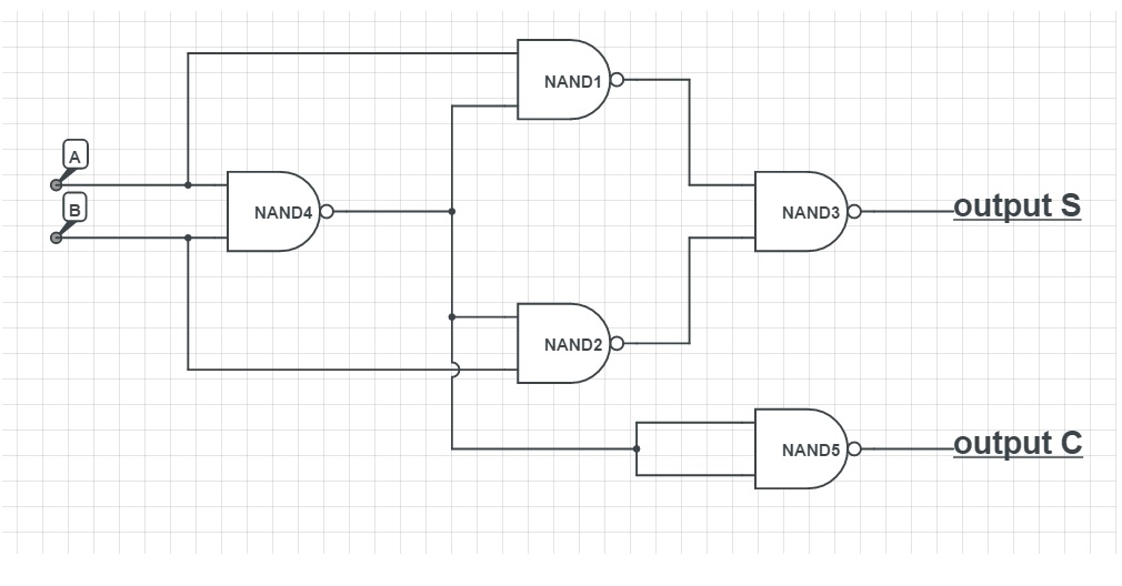
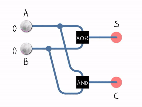
There are two elementary single-bit building blocks: the half adder and the full adder. A half adder combines two input bits to produce a sum bit and a carry bit. A full adder includes an extra input for a carry-in, allowing adders to be chained for multi-bit addition. At the logic-gate level a typical full adder can be implemented with two XOR gates, two AND gates, and one OR gate, arranged so that the XORs compute the sum bit and the AND/OR network computes the carry-out.
Common adder architectures
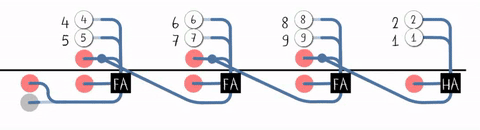
- Ripple-carry adder: Chains full adders so each carry-out becomes the next stage's carry-in. Simple and compact but carries "ripple" through every bit, which limits speed.
- Carry-lookahead adder: Uses extra logic to predict carries quickly, reducing delay at the cost of more gates and wiring.
- Carry-save and parallel adders: Employed in fast multipliers and arithmetic arrays to reduce the number of sequential carry operations.
Gate-level behaviour and truth
Conceptually, the sum bit is the XOR of the operand bits and the carry-in, while the carry-out is asserted when at least two of the three inputs are 1. In words: 0+0(+0) produces sum 0 and carry 0; 1+0(+0) yields sum 1 and carry 0; 1+1(+0) yields sum 0 and carry 1; and combining a carry-in can flip the sum and affect carry generation. Because carries can propagate from the least significant to the most significant bit, adders must balance size, complexity, and timing.
Worked example
To illustrate a ripple-carry addition, add the 4-bit numbers 1001 and 1100 (decimal 9 and 12). Beginning with the least significant bit: 1+0 = 1, carry 0. Next bit: 0+0 = 0, carry 0. Third bit: 0+1 = 1, carry 0. Most significant bit: 1+1 = 0 with carry 1. That final carry becomes a new most-significant digit, producing 10101 (decimal 21). This stepwise carry propagation is typical of simple chained adders; designs that reduce carry delay aim to perform these decisions in parallel or partially in advance.
Applications and notable considerations
Adders are fundamental in arithmetic logic units, digital signal processors, and hardware that implements multi-precision arithmetic. Designers choose an adder style based on a trade-off between silicon area, power consumption, and speed. In high-performance processors, carry-lookahead or more advanced prefix adders minimize latency; in resource-constrained devices, ripple-carry adders remain popular for their simplicity. For practical design and examples, see introductory resources such as basic arithmetic discussions and logic gate references like XOR, AND, and OR documentation.
Further study covers timing analysis, transistor-level implementations, and specialized multi-operand adders used in multiplication and accumulation. For more technical treatments and design patterns consult standard digital design references and tutorials at binary numbers and computer architecture resources.


Related articles
Author
AlegsaOnline.com Binary adder: digital circuits for adding binary numbers Leandro Alegsa
URL: https://en.alegsaonline.com/art/11579